A Speaker for High Fidelity Music and Electrifying Visuals
Project Motivation: With the lackluster performance of my cheap Bluetooth speaker and its 'temporary misplacement' in the garbage can, I was in the hunt for a new speaker. Going all-in, I wanted it to hit three needs: crisp sound, relatively loud volume, and jaw-dropping looks. Now, being an electrical engineer, I couldn't full-well just go out and buy one - where's the fun in that? So with the decision to make my own, I researched my options, and quickly realized that I didn't want the standard speaker set-up. That's just as boring as buying one off-the-shelf. So I thought about the more exotic, outlandish things that could make sound, and landed on the plasma arc speaker after being inspired by the laser show at a Zedd concert. After a Google search confirmed its practical use in some professional equipment today, and a guide to help me get started, I was sold.
Personal Objective: To build a wired speaker that can play music through the manipulation of plasma, a feat that is currently used in high-end tweeters in the music industry.
Skills learned: Basics of BJTs, MOSFETS, IGBTs, Audio Jacks, High Voltage Applications and Safety, Flyback Transformers, Plasma Conditions and Manipulation, External Power Supplies, and the 555 Timer. Upverter was the CAD software that I used.
The video above shows the plasma arc speaker in action. My phone's microphone didn't pick up all of the sound, so crank the volume up! How I made it and how it works are explained below.
How Does It Work? -------------- Instead of the traditional solid diaphragm that pulses in and out to create sound, a gaseous diaphragm composed of plasma is used instead. Because it has a much lower relative mass, it can vibrate much more quickly (less inertia!), allowing for sound at high frequencies to have much less distortion than traditional means.
Best Introduction to Plasma Physics that I've found online can be seen by clicking here.
It's not necessary for understanding the project, but it is provided for the curious mind.
For a complete Bill of Materials (BOM) incorporated into the PCB, please click here.
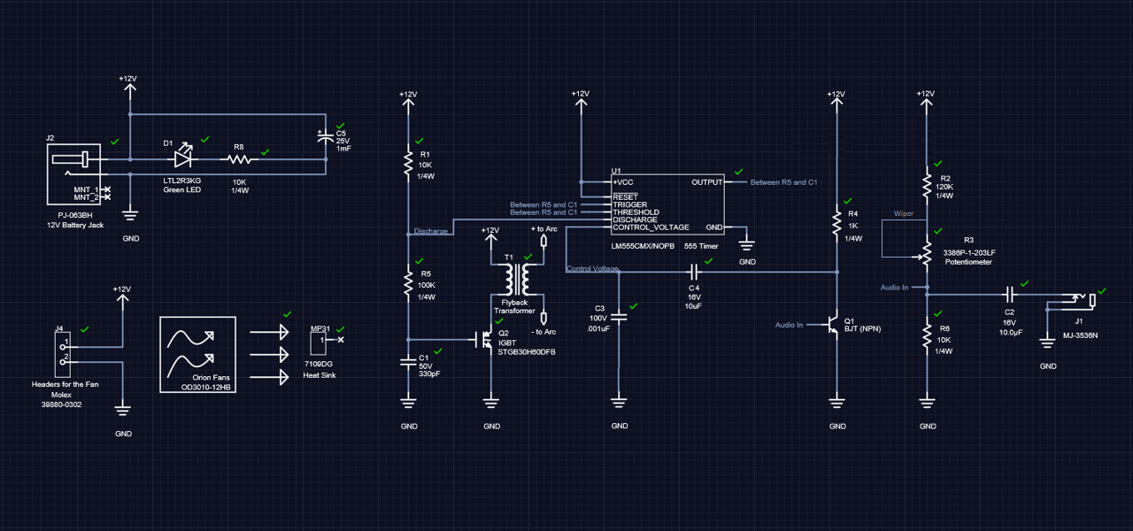
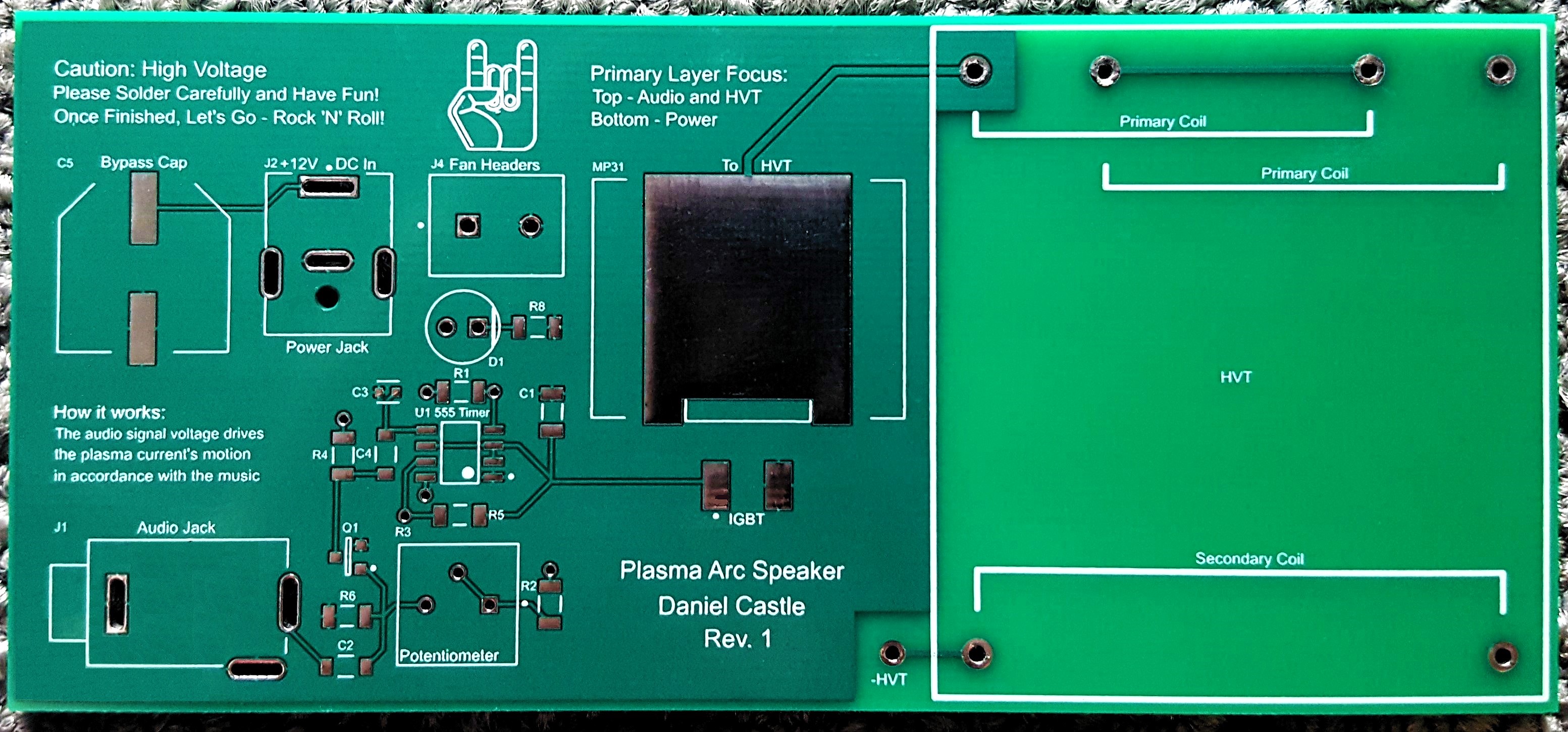
The image to the right is the schematic design of my PCB.
There are three main sections of the circuit - the power section [1], cooling section [2], and the frequency-modulating section [3].
[1] The power section is composed of a power jack, an LED for power indication, a resistor for the LED, a bypass capacitor to reduce any AC noise when turning on and off the power, and on the outside of the circuit, 8 1.5V AA batteries arranged in series, so that the total voltage output is 12V.
[2] The cooling section has three parts: the external fan, the headers providing power to that fan, and the heatsink attached to the insulated-gate bipolar transistor (IGBT), which is used in the circuit to rapidly switch the high voltage transformer on and off. Because the switching occurs so frequently, a lot of heat is generated, and both the heatsink and the fan are necessary to disperse the heat quickly into the surrounding air.
[3] The heart of the frequency-modulating section is the 555 Timer (designed by a fellow Northeastern alum back in the 70s - Go Huskies!). Set up in an astable mode to output an oscillation frequency that's dependent on an RC network of two resistors and a capacitor, it powers the rate at which the IGBT turns on the transformer. With a 'base frequency' of 22 kHz, the plasma arc doesn't produce any audible sound on its own, which would detract from the quality of the speaker.
Within the schematic, each section occupies its own space, allowing for easy reference in case any modifications are necessary. Using flags and appropriately-named lines, each element could be wired together virtually, without the need to clutter the board with excessive, redundant, and explicitly-defined lines that criss-cross the entire schematic.
Once the components were selected and connected via nets, their footprints were then generated and manipulated to achieve the right position, spacing, and orientation on the board.
The image to the right shows the design of the top layer of my PCB.
In my 2-layer board, the top layer was primarily focused on providing the audio voltage signals that are driving the vibrating plasma current.
From the audio jack, the signals first pass through a blocking capacitor to remove any DC or lower frequency noise, ensuring that only higher frequencies get through.
The next step is to fine-tune the audio signals' bias to the NPN transistor amplifier using the potentiometer. It's important to remember that bipolar junction transistors (BJTs), which are built to process time-varying (AC) signals, also require a steady (DC) voltage to operate correctly - in other words, a bias, which ensures that stable current levels are applied to the BJT in all conditions. Those AC signals are then superimposed onto the DC bias voltage, and by doing so, a higher fidelity signal, with no clipping, can be achieved. When first using the speaker, the potentiometer should be at its midpoint position, and can be further manipulated using a small screw to make the signals sharper if necessary.
With the current values of R1, R5, and C1, the base frequency of the plasma vibrations will be 22 KHz, and in this set-up, the plasma arc will be silent when running (20kHz is around the maximum frequency that the ear can hear). By varying the voltage on the control pin of the 555 timer, the output of the IGBT can be varied independently from the base frequency of the RC network, creating a frequency-modulated signal. After sound (varying AC voltage) is played through the audio jack, this FM signal, after a massive voltage amplification by the transformer, drives the plasma to jiggle in tandem with the audio. Because the IGBT is central to the performance of the high voltage transformer, I'll explain it in more detail below.
Check out the image below for the basic model and circuit symbol of the IGBT:
The IGBT is a three terminal device that combines the properties of MOSFET with a BJT, typically in a configuration with an insulated gate N-channel MOSFET at the input and a PNP bipolar transistor as the output. As a result, the terminals are labeled as: Collector, Emitter, and Gate. Two of its terminals (C-E) are associated with amplifying current, while its third terminal (G) controls the device.
The amount of amplification achieved by the insulated gate bipolar transistor is a ratio between its output signal and its input signal. In other words, it's a voltage-controlled device, and in fact, it only needs a small voltage to maintain current flow. That current flow is also unidirectional, flowing from the collector to the emitter only, unlike a MOSFET, which has bidirectional current switching capabilities. With its high input impedance, low output impedance, and fast switching between HIGH and LOW states, it makes a great choice for most KHz frequency applications.
This speaker, with the small amount of plasma generated, is more similar to a tweeter than a full-fledged bass. It is better at producing higher frequency sound than lower frequency sound, because a larger plasma arc would be able to push more air molecules, which makes more of a difference on the lower end of the hearing range.
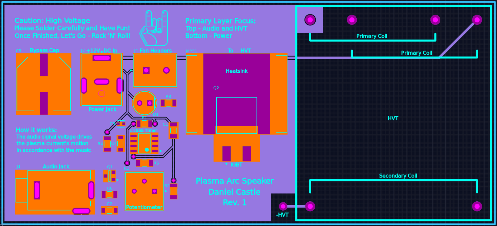
The image to the right shows the design of the bottom layer of my PCB.
In my 2-layer board, the bottom layer was primarily focused on providing power to the board.
From the 12V DC power jack (powered by 8 AA batteries connected in series), a large trace leads directly to one of the pins of the high voltage transformer (HVT). The rest of the traces lead to a bypass capacitor to filter AC noise, an LED to indicate that the board has power, and the components associated with running the 555 timer, as well as the 555 timer itself.
As the 555 timer is a central component of the speaker, some time should be spend understanding what it is and how it works on a more detailed level. The single 555 Timer chip in its basic form is an 8-pin Dual-in-line Package (DIP) device consisting of 25 transistors, 2 diodes, and 16 resistors arranged to form two comparators, a flip-flop, and an output stage that can source or sink a relatively high current (up to 200mA). Because it can be used in a variety of timer, pulse generation, and oscillator applications, it's an extremely popular IC, with over 1 billion chips having been made worldwide.
The most common use of the 555 timer oscillator is as a simple astable oscillator, created by connecting two resistors and a capacitor to three of its pins (Trigger, Threshold, and Discharge) to generate fixed pulses with a time period determined by the time constant of the RC network. Astable just means there's an automatic built-in triggering mechanism that switches between two unstable states, without the need for an external trigger. This set-up is what I used in my circuit. More on how it works is explained below.
Check out the image below for the block diagram of the chip:
How Astable Mode Works
[-] Pin 2 - Trigger: Turns on the output when the voltage supplied to it drops below 1/3 of Vcc
[-] Pin 6 - Threshold: Turns off the output when the voltage supplied to it reaches above 2/3 Vcc
[-] Pin 7 - Discharge: When the output voltage is low, it discharges C1 to ground.
In astable mode, the output cycles on and off continuously. In the PCB schematic, notice that the threshold pin and the trigger pin are connected to C1. This makes the voltage the same at the trigger pin, threshold pin, and C1.
At the beginning of an on/off cycle, the voltage is low at C1, the trigger pin, and the threshold pin. Whenever the trigger pin voltage is low, the output is on, and the discharge pin is off. Since the discharge pin is off, current can flow through resistors R1 and R2, charging capacitor C1.
Once C1 charges to 2/3 Vcc, the output is switched off by the threshold pin. When the output goes off, the discharge pin switches on. This switch allows the charge accumulated on capacitor C1 to drain to ground.
Once the voltage across C1 drops below 1/3 Vcc, the trigger pin turns off the discharge pin, so C1 can start charging again. And the cycle repeats, with the input to the IGBT connected to the same line and oscillating as well.
--------------
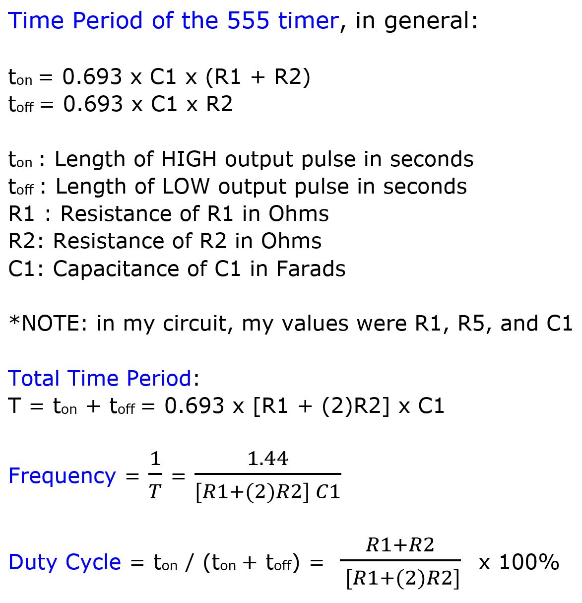
Check out the image below for how I calculated my base frequency of around 22 KHz:
555 Timer Equations
To get the base frequency of around 22 KHz, the equations shown above were used.
When charging the capacitor, both resistors are used, but when discharging the capacitor (enabled through the DISCHARGE pin), only R2 (in my circuit, R5) is used. Therefore, the time periods for ON and OFF are different.
I started by picking a capacitor value, as there are relatively fewer values for capacitors than resistors. Once I chose that value, which needed to have a lower capacitance than typical capacitor values to create smaller RC time periods, I chose a large R2 value, as having a much larger R2 value than an R1 value (therefore giving close to a 50% duty cycle) is standard practice for the 555 timer. In addition, the IGBT I chose has a much faster switching rate than a audio signal would provide, so there was no need to do something atypical in this case. The last requirement was that R1 provided a value such that the base frequency would be close to 22 KHz, and with the combination of 330pF for C1, 100,000 Ohms for R2, and 1,000 Ohms for R1, the math lined up to be 21.77 KHz, which I considered close enough.
It's worth noting that the duty cycle will always be greater than 50%, as the ON time is greater than the OFF time. To get a lower duty cycle, a diode would be needed to circumvent R2 during the charging cycle.
--------------
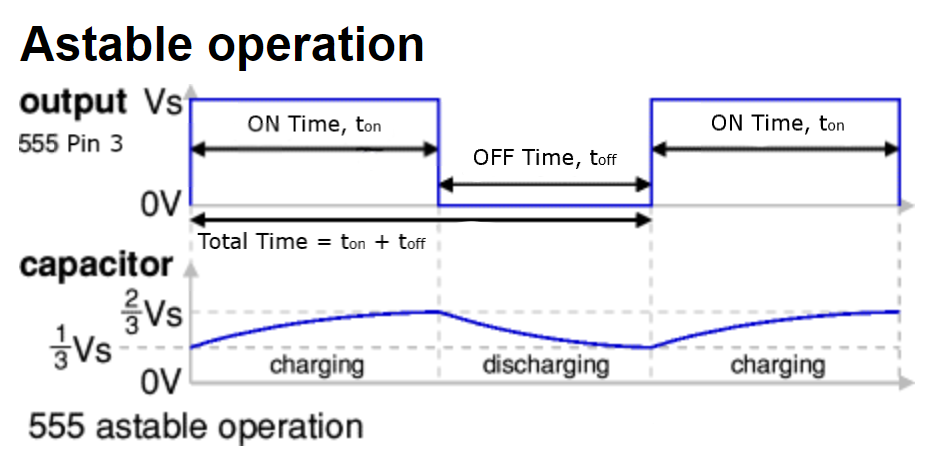
Check out the image below for what the output of the 555 timer looks like:
555 Timer Astable Operations
The two comparators within the chip produce an output voltage dependent upon the voltage difference at their inputs, which is determined by the charging and discharging action of the externally connected RC network (the astable configuration as mentioned above). The outputs from both comparators are connected to the two inputs of the flip-flop, which in turn produces either a "HIGH" or "LOW" level output at Q based on the states of its inputs. The output from the flip-flop is then able to source or sink the connected load by producing either a "HIGH" or "LOW" voltage level at the output driver circuit within the chip.
--------------
Linking it back to my circuit
Technically, the plasma is created through the large voltage potential between the two ends of the HVT, which is driven by the IGBT. The IGBT, in turn, is driven by the 555 timer, which is operated as shown above.
The waveforms of the circuit look something like this: audio signal (sinusoidal) -> 555 timer output (square waves) -> IGBT output (square waves) -> HVT output (sawtooth waves). The high voltage transformer is explained in the next section.
While plasma is defined more fully than simply "ionized gas", that definition is sufficient here to understand the system. Please keep in mind that using this plasma speaker creates ozone as a byproduct of heating the air, which is dangerous at high levels. Don't leave the speaker running for a long time, unless it has proper ventilation or housing to limit exposure.
The image to the right shows the top layer of my PCB, straight from the manufacturer, Sunstone Circuits.
With the dimensions of 124mm x 56mm, the board is a little smaller than the Galaxy S6 phone from Samsung.
The silkscreen shows which components go on the board, and where they need to be soldered. Makes life a little easier than scrutinizing schematics and comparing part numbers, so it was definitely well worth it.
On the board, most of the components used pads, with little room for using a traditional soldering iron. Therefore, I used my trusty solder paste to attach them to the board.
Speaking of the board, the largest individual component by far is the high voltage transformer. Because its operation is so important to this device, some time should be taken here as well to understanding its usage.
So let's elaborate. The transformer that I used was a flyblack transformer, which is a special kind of transformer that generates high voltage sawtooth signals at a relatively high frequencies (15 - 50 KHz). Originally developed for cathode ray tube (CRT) TVs, its trick is that, unlike conventional transformers, a flyback transformer is not fed with a signal of the same waveform (a switched DC voltage signal) as the intended output current (sawtooth).
So, how does it work? Well, the primary winding of the flyback transformer is driven by a switch (the IGBT in this device). When the switch is turned on, the primary inductance causes the current to build up in a ramp, and the magnetic field around the winding increases. When the switch is turned off, the current in the primary drops to zero, and the energy stored in the magnetic field is released to the secondary as the field collapses. The voltage in the secondary winding rises very quickly (usually less than a microsecond) until it is limited by the load. Once the voltage reaches a sufficient level as to allow the secondary current to flow, the current decreases in the form of a descending ramp.
Check out the image below for what an example flyback transformer output would look like:
Flyback Transformer Example Waveforms
The flyback transformer in my case operates in discontinuous mode, meaning that the secondary current is allowed to discharge completely to zero (no energy is left over in the core during ON times of the IGBT). There is also a continuous mode, when some energy is always stored in the core (and the secondary current waveforms look trapezoidal rather than triangular).
Because I wanted the speaker to be as high fidelity as possible, I wanted to ensure that the sound coming from the speaker wouldn't have a "base volume" that would be the result of a continuous mode setup, as low volume would sound closer to high volume on a given soundtrack. That's why I chose the discontinuous mode, which would give me a higher volume range.
--------------
The specific flyback transformer that I used has two primaries, which were connected in series to avoid saturating the shared core within both of the primaries, as any amount of DC voltage dropped across the primary windings (12V in this case) will cause additional magnetic flux in the core. Since more flux in the primaries leads to a higher voltage in the secondary, and the voltage drop between the primaries helps to spread the heat between the windings and minimize energy losses, I thought it prudent to go ahead and wire them as I did.
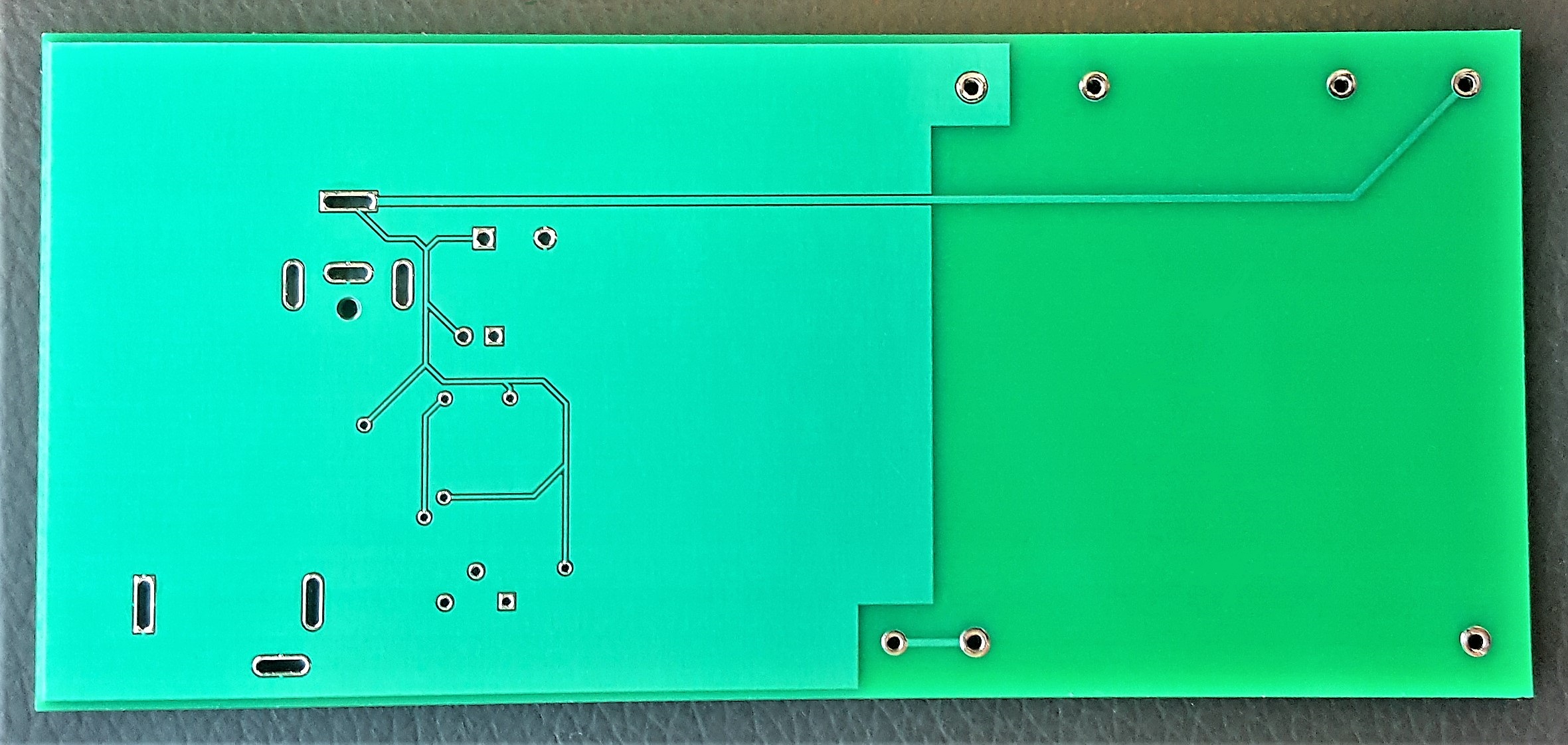
The image to the right shows the printed bottom layer of the PCB.
As mentioned above, these traces focused on providing power to the various components. For those that are surface mounted, vias are used to connect the traces to the top layer.
The large ground pour is clearly visible here, as well. Notably, it is not under the high voltage transformer, to prevent any leakage flux from affecting the reference voltage (which is what ground really is).
The image to the right shows the top layer of my PCB, with the components soldered on.
The audio jack on the bottom left is connected to the MP3 player on the far right. Once I choose my song and click "Play", and the power is turned on, I'm good to go!
To ensure that no accidental shocks could occur while I'm not using the device, keep in mind that the power jack is disconnected here though, just to be clear.
The heatsink covers the IGBT on top and is connected by copper on the bottom to the collector. With the action of the fan (the rock-and-roll hand sign serving to point to the fan as well as look cool), the IGBT stays nice and cool, or more accurately room-temperature.
The two leads on the bottom are from the transformer, and they influence where the magic happens - those are the 22 gauge high voltage wires that lead to the plastic container where the plasma is generated.
The image to the right shows the running plasma speaker, playing "Born to be Wild" by Steppenwolf.
The air over the speaker does get pretty hot, just FYI for anyone who wants to take a similar picture.
Adjustment of the inner wire was necessary to get a clear sound. If the speaker starts to crawl up the sides of the wire, the sound will be distorted, so proper wire form, with the ends pointing toward each other, is essential.
The volume of the MP3 player may also need to be adjusted too. 75-100mV is around what mine was putting out to get a nice signal, but it depends on the potentiometer resistance as well.
The sound wasn't as full as I had hoped - with the small arc, there wasn't much air that was vibrating, so the volume wasn't very loud. I'd put it at a quarter the volume of my Galaxy S6 Active phone, so hearing it by itself is fine, but perhaps not during a normal conversation with other people.
Because the clearest sound happens when the speaker arc stream is constant with respect to a certain frequency, the crazy visuals that I was kinda hoping to see ended up being counter to the main goal of hearing good music. In other words, the speaker performs better when the arc looks less like lightning and more like an LED, so it's still cool to look at in the dark, but maybe not jaw-dropping.
It was a fun project overall, though! I'd improve it in the future by using a higher-rated HVT and IGBT (which would allow more current and more airflow, which would lead to a higher volume), or spending more time adjusting the wires to get the cleanest signal possible.
 The image to the right is the schematic design of my PCB.
 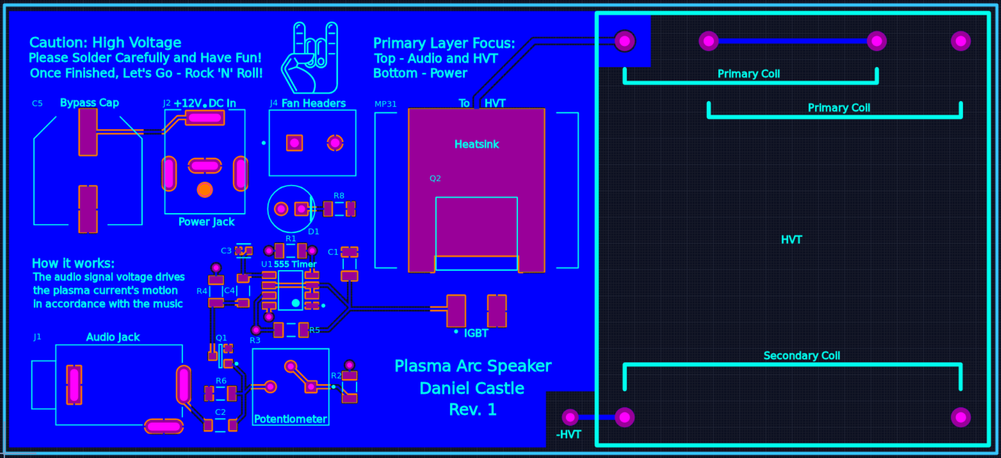 The image to the right shows the design of the top layer of my PCB.
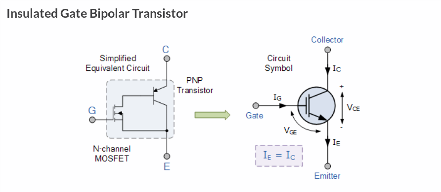
 The image to the right shows the design of the bottom layer of my PCB.
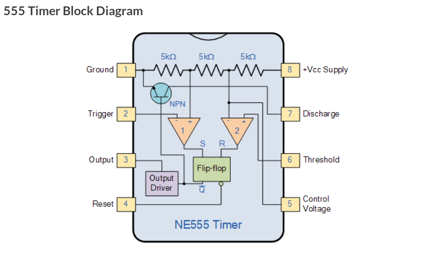
 The image to the right shows the top layer of my PCB, straight from the manufacturer, Sunstone Circuits.
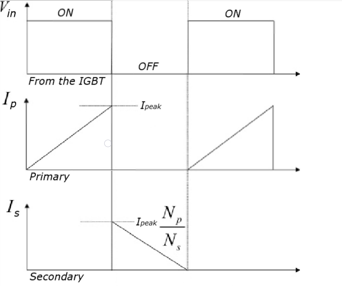
 The image to the right shows the printed bottom layer of the PCB.
 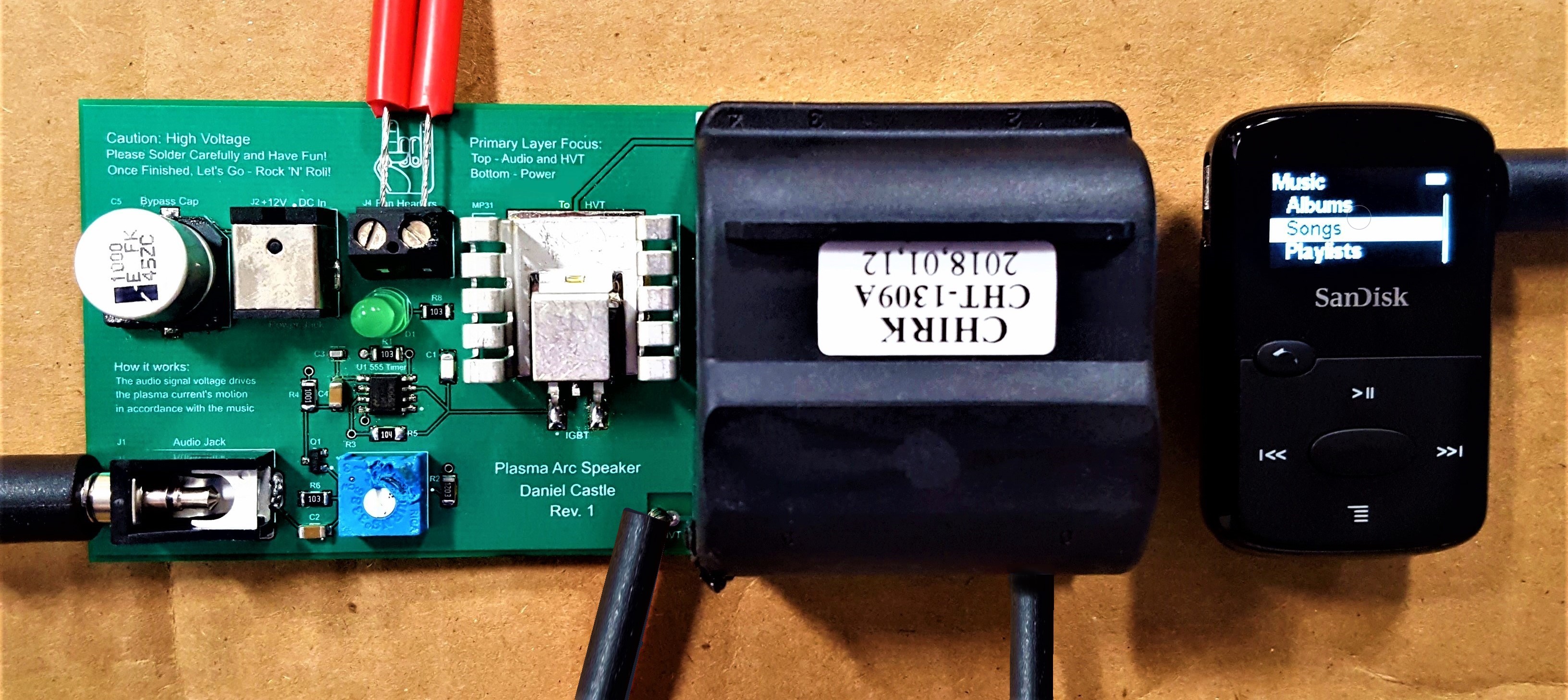 The image to the right shows the top layer of my PCB, with the components soldered on.
 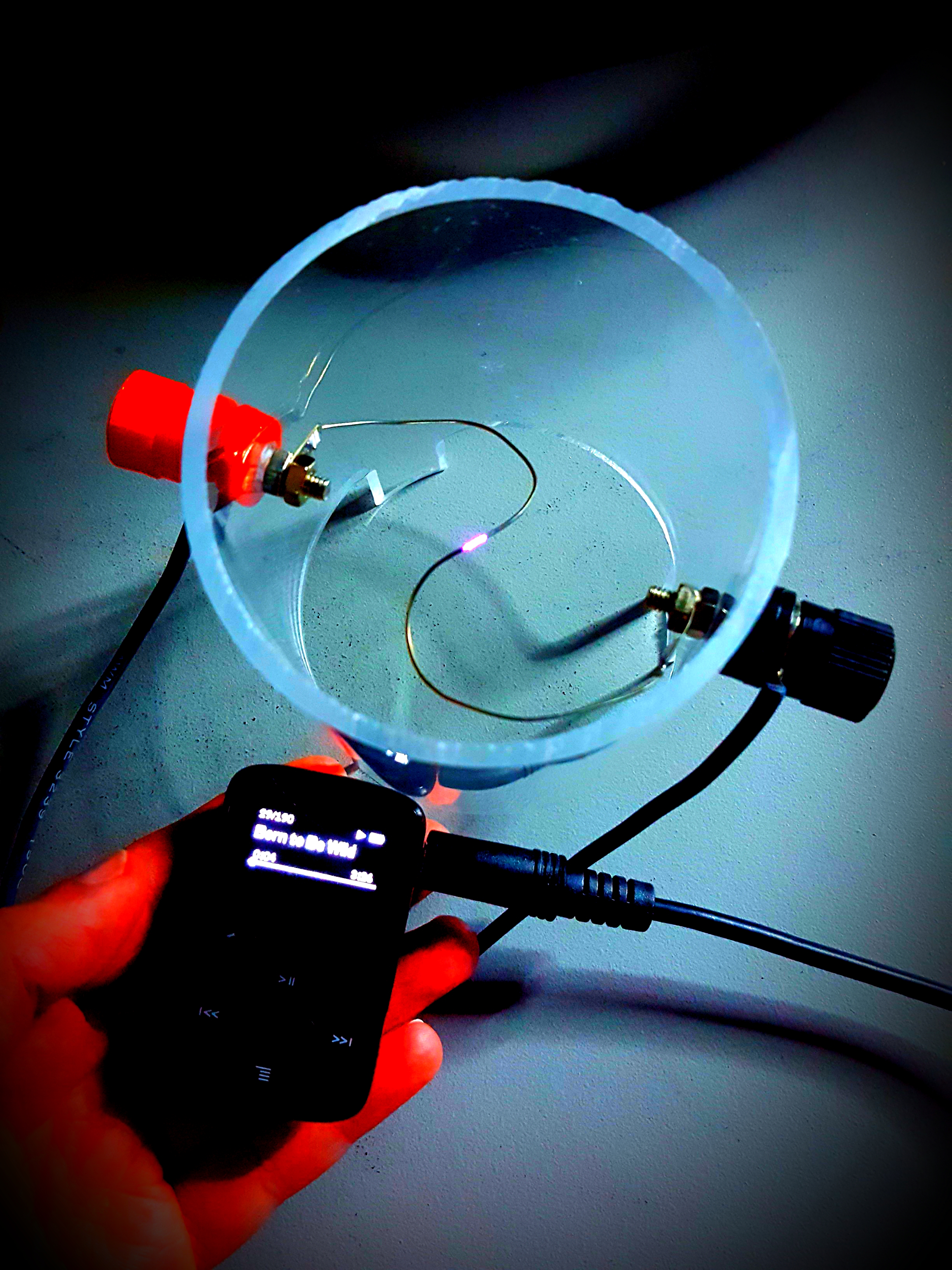 The image to the right shows the running plasma speaker, playing "Born to be Wild" by Steppenwolf.